
- within Coronavirus (COVID-19), Criminal Law and Real Estate and Construction topic(s)
Today, Yangtze Memory technologies is not new to anyone in the memory industry. Yangtze River Storage Technology Co., Ltd. (YMTC) was established in July 2016 and is headquartered in Wuhan. It is an integrated device manufacturer (IDM) that Designs, Manufactures, and Sells 3D NAND flash memory.
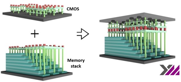
YMTC first marked its presence in the global memory market in 2017 when it announced that they have designed China's first 3D NAND flash memory through collaborations. However, the name YMTC became significant in global memory market in September 2019, when YMTC started mass production of 64-layer TLC 3D NAND flash memory equipped with YMTC's independently designed and owned Xtacking" architecture. Xtacking is a propriety YMTC innovation to manufacture the memory and the logic circuits on separate wafers and connect them using plasma activation and thermal annealing.
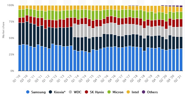
YMTC took a big leap in April 2020, when it announced industry's first 128-layer QLC flash memory that has the highest IO speed, highest storage density and highest single Capacity. As per the latest news, YMTC has already started production of 128-Layer, 3D QLC NAND and are supposed to hit the market sooner. NAND flash manufacturers revenue share worldwide from 2010 to 2021, by quarter indicates that Samsung is the undisputed leader in this industry segment.
Source: www.statista.com
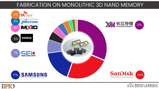
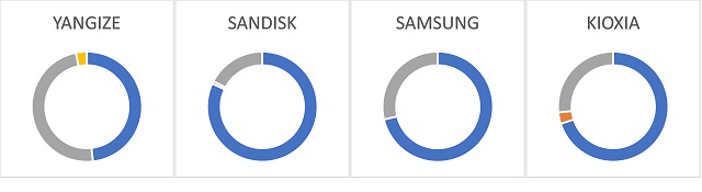
However, an analysis of worldwide patents related to the fabrication of Monolithic 3D NAND memory published after Jan 2018 shows that YMTC is set to disrupt this industry with its propriety Xtacking" technology. YMTC gave a clear hint about this in 2020 when it unveiled 128 Layer 3D NAND memory. Since its inception, YMTC has invested heavily in R&D activities and has filed close to 4000+ patent in memory space. Interestingly, considering the patents published since Jan 2018, YMTC has surpassed industry leaders in securing key technologies related to fabrication of monolithic 3D NAND memory module. Around 1/3rd of the patents published since Jan 2018 that explicitly relate to fabrication of monolithic 3D NAND memory are assigned to Yangtze Memory Technologies, followed by SanDisk [now a apart of Western Digital] and Samsung.
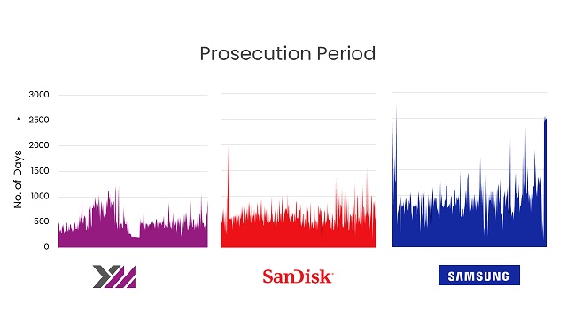
YMTC has already hinted that in coming years, they have plans to monetize their intellectual property in this space by licensing out their proprietary monolithic 3D NAND fabrication technologies to players like Samsung and Micron. YMTC is not only frequently filing patents but a quick look into the prosecution timeline of 3D NAND fabrication-related patents granted to the top 3 patent holding entities since Jan 2018 suggests that Yangtze Memory Technologies has obtained most of its patent rights in less than 500 days, either due to strong innovation or due to China's patent policy.
In addition to this, close to 50% of the patent families published by Yangtze Memory Technologies is still under prosecution which suggest that the base technology on which YMTC is working isn't saturated yet and a lot newer improvement/ continuation patents will be seen in coming days. On the other hand, an analysis of count of pending patents assigned to other key players indicates that they are working at a slower pace or working on technologies that are the are the verge of saturation.
YMTC is not only securing fresh patents in 3D NAND fabrication space but has plans to in-license few of the best available technologies in the market that would add value and efficiency to the YMTC memory streak. Recently, YMTC has obtained access to access to a foundational portfolio of Xperi's DBI hybrid bonding technology. As per a Senior VP at Xperi, "DBI hybrid bonding is a key enabling technology for current and future generations of high performance, high-capacity 3D NAND flash memory. We are proud to provide YMTC access to our foundational IP portfolio and look forward to further expanding our relationship".
Though Kioxia and Western Digital are a tough competition for YMTC and have also announced that the companies have developed their sixth-generation, 162-layer 3D flash memory technology based on a new split-gate architecture. The new device will likely stack two 80-layer structures on top of each other, forming a 160-layer device. Yet looking at the technology acquisition rate, it seems like they need to speed up their R&D activities.
While the global storage leader Samsung has moved their R&D onto the 8th generation V-NAND platform by stacking 200 layers or above, their US rival Micron has recently announced a new 3D flash memory technology, which has an astonishing 176 layers of memory cells stacked on top of each other.
Tough the future path is tough for YMTC, yet they are on the track and have already started the production of 128-Layer, 3D QLC NAND memory and has plans to transition to its Xtacking 3.0 design sometime in the latter half of 2022.
It would be interesting to revisit the NAND flash manufacturers revenue analysis graph once the YMTC's 3D NAND memory modules becomes commercially available in the market.
Why Yangtze Memory Technologies Poised To Lead The Future Memory Market?
The content of this article is intended to provide a general guide to the subject matter. Specialist advice should be sought about your specific circumstances.
[View Source]